- 您现在的位置:买卖IC网 > Sheet目录3873 > PIC18F45K20-I/MV (Microchip Technology)MCU 32KB FLASH 1536B RAM 40-UQFN
2007 Microchip Technology Inc.
Preliminary
DS70165E-page 173
dsPIC33F
TABLE 14-1:
EXAMPLE PWM FREQUENCIES AND RESOLUTIONS AT 4 MIPS (FCY = 4 MHz)
TABLE 14-2:
EXAMPLE PWM FREQUENCIES AND RESOLUTIONS AT 16 MIPS (FCY = 16 MHz)
TABLE 14-3:
EXAMPLE PWM FREQUENCIES AND RESOLUTIONS AT 40 MIPS (FCY = 40 MHz)
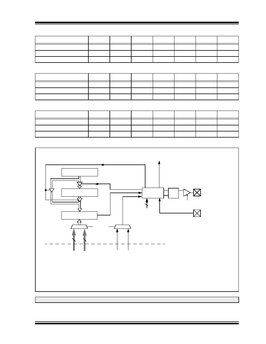
FIGURE 14-1:
OUTPUT COMPARE MODULE BLOCK DIAGRAM
PWM Frequency
7.6 Hz
61 Hz
122 Hz
977 Hz
3.9 kHz
31.3 kHz
125 kHz
Timer Prescaler Ratio
8
1
111
11
Period Register Value
FFFFh
7FFFh
0FFFh
03FFh
007Fh
001Fh
Resolution (bits)
16
15
12
10
7
5
PWM Frequency
30.5 Hz
244 Hz
488 Hz
3.9 kHz
15.6 kHz
125 kHz
500 kHz
Timer Prescaler Ratio
8
1
111
11
Period Register Value
FFFFh
7FFFh
0FFFh
03FFh
007Fh
001Fh
Resolution (bits)
16
15
12
10
7
5
PWM Frequency
76 Hz
610 Hz
1.22 Hz
9.77 kHz
39 kHz
313 kHz
1.25 MHz
Timer Prescaler Ratio
8
1
111
11
Period Register Value
FFFFh
7FFFh
0FFFh
03FFh
007Fh
001Fh
Resolution (bits)
16
15
12
10
7
5
Note:
Only OC1 and OC2 can trigger a DMA data transfer.
OCxR(1)
Comparator
Output
Logic
OCM2:OCM0
Output Enable
OCx(1)
Set Flag bit
OCxIF(1)
OCxRS(1)
Mode Select
3
Note 1:Where ‘x’ is shown, reference is made to the registers associated with the respective output compare channels 1
through 8.
2: OCFA pin controls OC1-OC4 channels. OCFB pin controls OC5-OC8 channels.
3: Each output compare channel can use one of two selectable time bases. Refer to the device data sheet for the
time bases associated with the module.
OCTSEL
0
1
16
OCFA or OCFB(2)
TMR register inputs
from time bases(3)
Period match signals
from time bases(3)
0
1
Q
S
R
发布紧急采购,3分钟左右您将得到回复。
相关PDF资料
PIC16CR76T-I/SS
IC PIC MCU 8KX14 28SSOP
PIC18F13K50-I/P
IC PIC MCU FLASH 4KX16 20-PDIP
PIC16CR76T-I/SO
IC PIC MCU 8KX14 28SOIC
PIC18LF24K22-I/MV
IC PIC MCU 16KB FLASH 28UQFN
PIC18LF24K22-I/ML
IC PIC MCU 16KB FLASH 28QFN
PIC16CR76T-I/ML
IC PIC MCU 8KX14 28QFN
PIC16F627-04/P
IC MCU FLASH 1KX14 COMP 18DIP
PIC18F45J10-I/ML
IC PIC MCU FLASH 16KX16 44QFN
相关代理商/技术参数
PIC18F45K20-I/P
功能描述:8位微控制器 -MCU 32KB Flash 1536B RAM 25 I/O 8B RoHS:否 制造商:Silicon Labs 核心:8051 处理器系列:C8051F39x 数据总线宽度:8 bit 最大时钟频率:50 MHz 程序存储器大小:16 KB 数据 RAM 大小:1 KB 片上 ADC:Yes 工作电源电压:1.8 V to 3.6 V 工作温度范围:- 40 C to + 105 C 封装 / 箱体:QFN-20 安装风格:SMD/SMT
PIC18F45K20-I/PT
功能描述:8位微控制器 -MCU 32KB Flash 1536B RAM 25 I/O 8B RoHS:否 制造商:Silicon Labs 核心:8051 处理器系列:C8051F39x 数据总线宽度:8 bit 最大时钟频率:50 MHz 程序存储器大小:16 KB 数据 RAM 大小:1 KB 片上 ADC:Yes 工作电源电压:1.8 V to 3.6 V 工作温度范围:- 40 C to + 105 C 封装 / 箱体:QFN-20 安装风格:SMD/SMT
PIC18F45K20T-I/ML
功能描述:8位微控制器 -MCU 32KB Flash 1536B RAM 25 I/O 8B RoHS:否 制造商:Silicon Labs 核心:8051 处理器系列:C8051F39x 数据总线宽度:8 bit 最大时钟频率:50 MHz 程序存储器大小:16 KB 数据 RAM 大小:1 KB 片上 ADC:Yes 工作电源电压:1.8 V to 3.6 V 工作温度范围:- 40 C to + 105 C 封装 / 箱体:QFN-20 安装风格:SMD/SMT
PIC18F45K20T-I/MLV01
制造商:Microchip Technology Inc 功能描述:
PIC18F45K20T-I/MV
功能描述:8位微控制器 -MCU 32KB FL 1536b RAM 8b Familynanowatt XLP
RoHS:否 制造商:Silicon Labs 核心:8051 处理器系列:C8051F39x 数据总线宽度:8 bit 最大时钟频率:50 MHz 程序存储器大小:16 KB 数据 RAM 大小:1 KB 片上 ADC:Yes 工作电源电压:1.8 V to 3.6 V 工作温度范围:- 40 C to + 105 C 封装 / 箱体:QFN-20 安装风格:SMD/SMT
PIC18F45K20T-I/PT
功能描述:8位微控制器 -MCU 32KB Flash 1536B RAM 25 I/O 8B RoHS:否 制造商:Silicon Labs 核心:8051 处理器系列:C8051F39x 数据总线宽度:8 bit 最大时钟频率:50 MHz 程序存储器大小:16 KB 数据 RAM 大小:1 KB 片上 ADC:Yes 工作电源电压:1.8 V to 3.6 V 工作温度范围:- 40 C to + 105 C 封装 / 箱体:QFN-20 安装风格:SMD/SMT
PIC18F45K22-E/ML
功能描述:8位微控制器 -MCU 32KB Flash 1536B RAM 8B nanoWatt RoHS:否 制造商:Silicon Labs 核心:8051 处理器系列:C8051F39x 数据总线宽度:8 bit 最大时钟频率:50 MHz 程序存储器大小:16 KB 数据 RAM 大小:1 KB 片上 ADC:Yes 工作电源电压:1.8 V to 3.6 V 工作温度范围:- 40 C to + 105 C 封装 / 箱体:QFN-20 安装风格:SMD/SMT
PIC18F45K22-E/MV
功能描述:8位微控制器 -MCU 32KB 1536b RAM 8bit familynanoWatt XLP RoHS:否 制造商:Silicon Labs 核心:8051 处理器系列:C8051F39x 数据总线宽度:8 bit 最大时钟频率:50 MHz 程序存储器大小:16 KB 数据 RAM 大小:1 KB 片上 ADC:Yes 工作电源电压:1.8 V to 3.6 V 工作温度范围:- 40 C to + 105 C 封装 / 箱体:QFN-20 安装风格:SMD/SMT